1 / 5
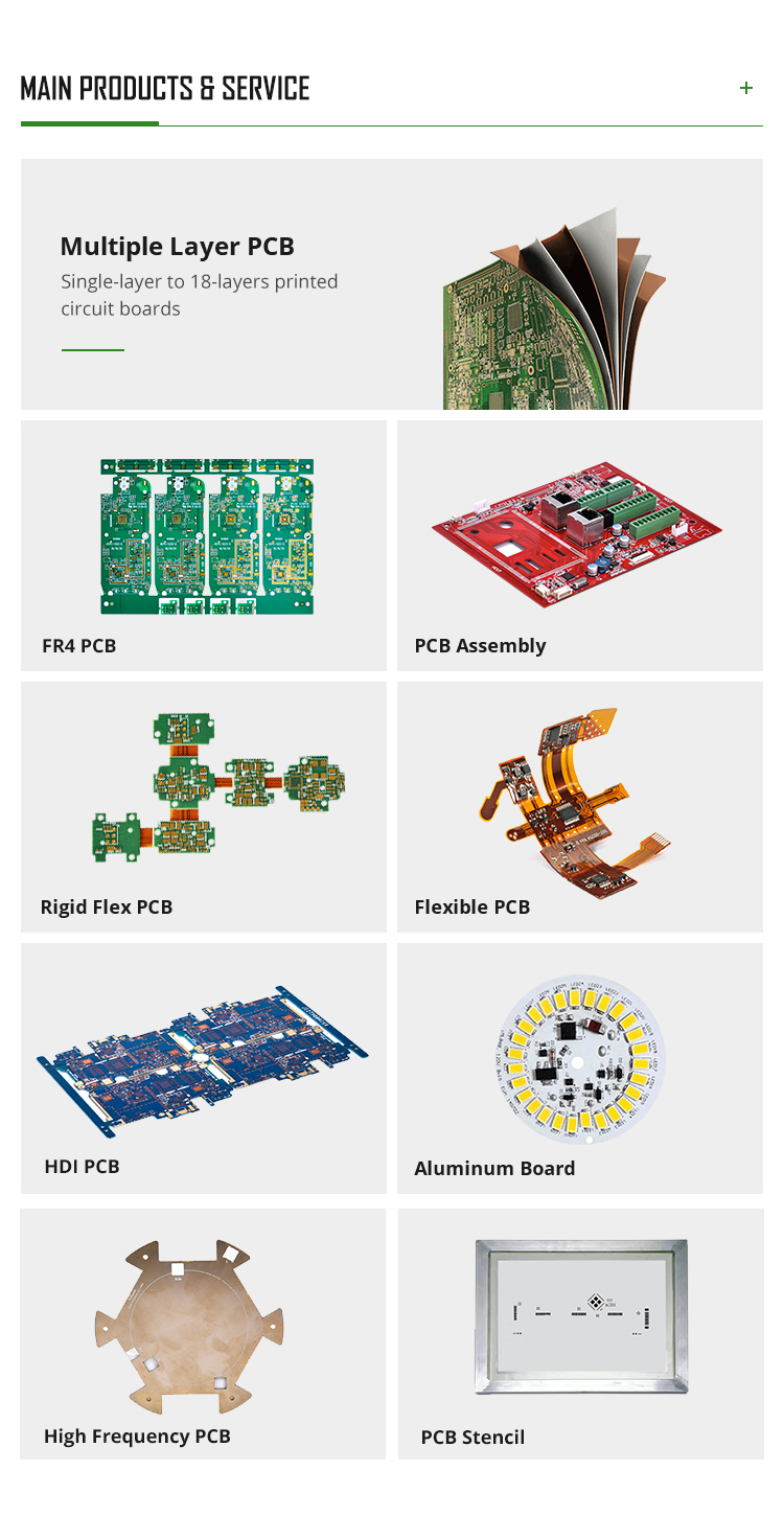

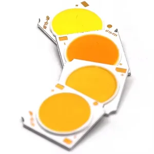
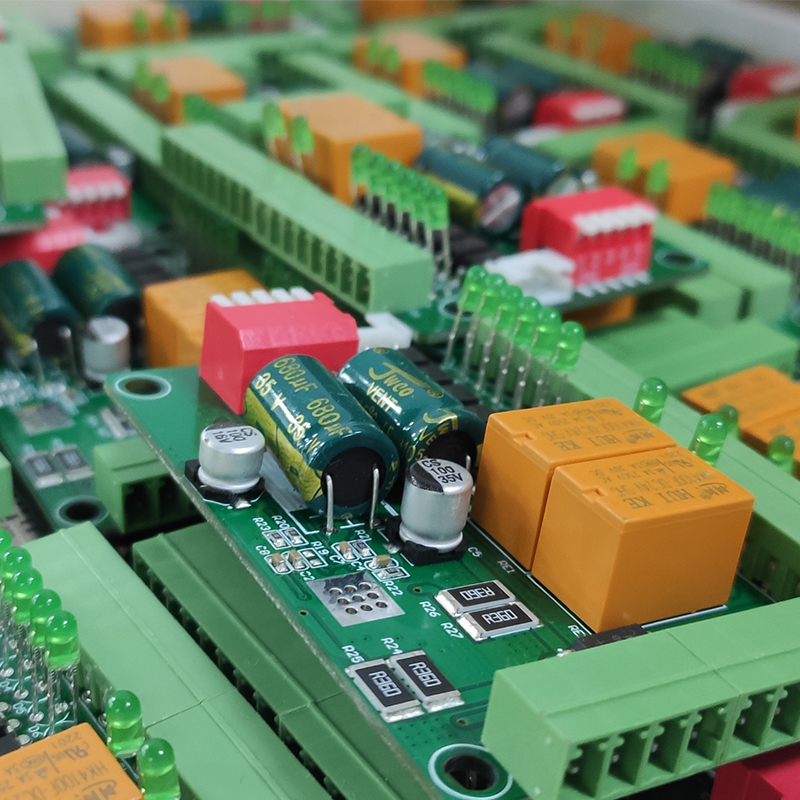
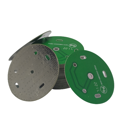
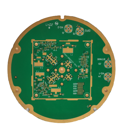
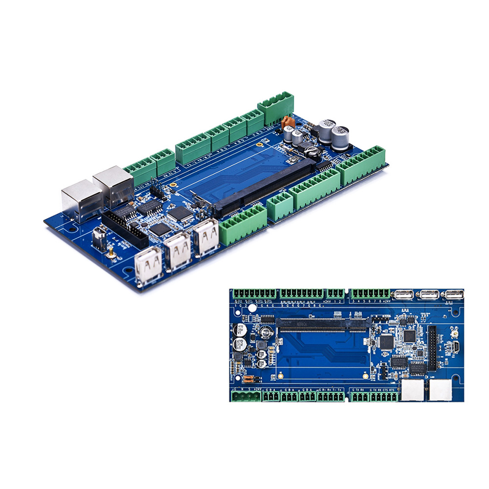
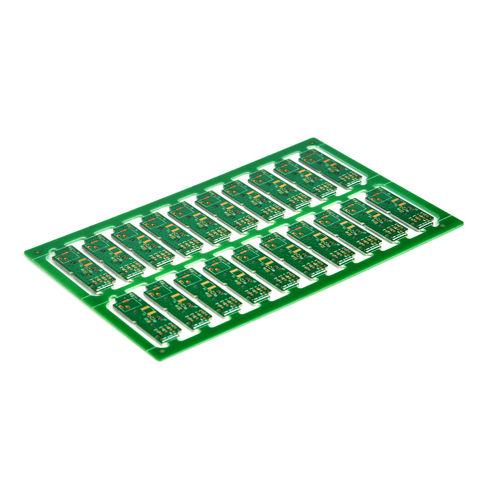
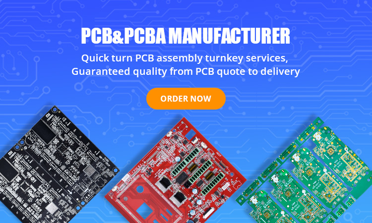
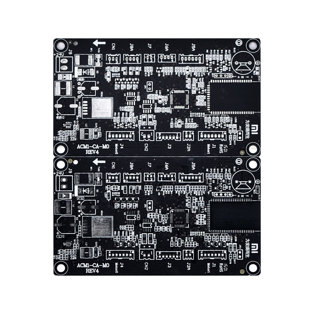
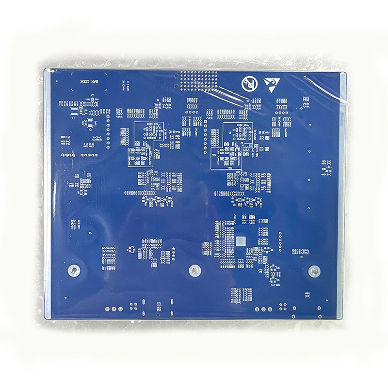
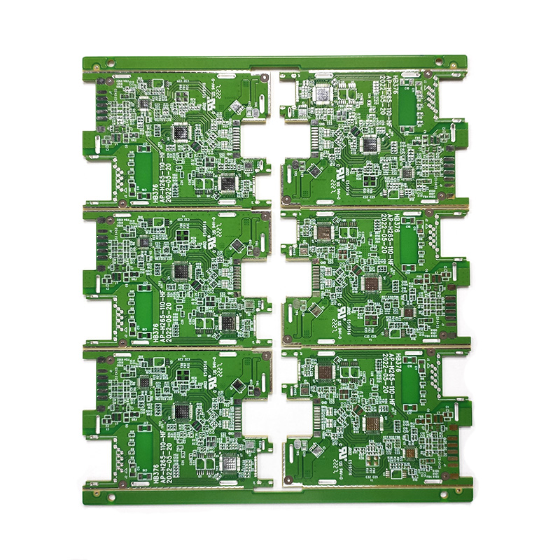
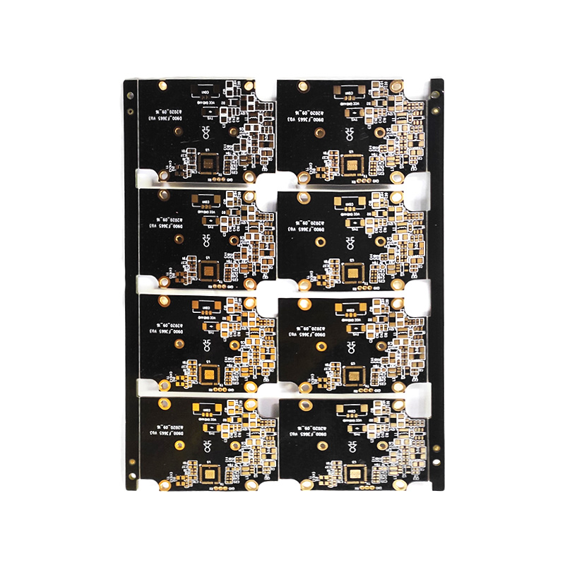
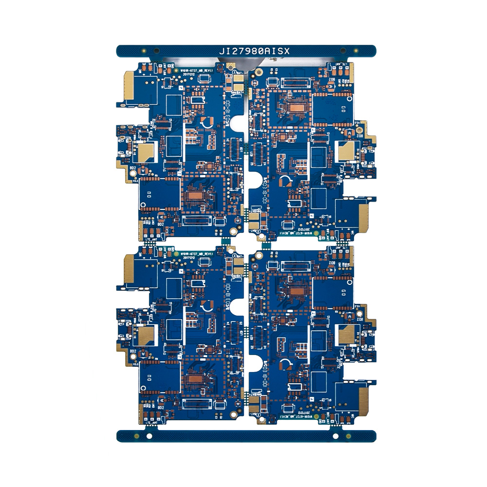
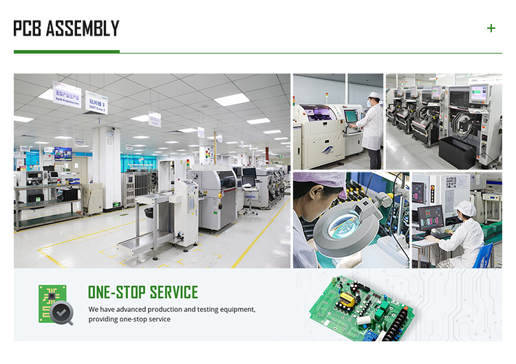
PCB is a Printed Circuit Board. It's an important electronic component, which is a support for electronic components and a carrier for electrical connections between electronic components. Rigid circuit boards are very popular largely due to their low cost. In conventional electronics, and particularly in consumer electronics, with greater space availability, manufacturers can save significantly by using rigid circuit boards. However, flexible PCBs are beginning to siphon market share from rigid circuit boards due to their versatility, among other advantages. PCBA is the whole manufacturing process of PCB bare board by SMT feeding and DIP plug-in.
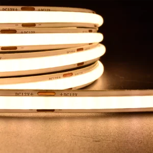
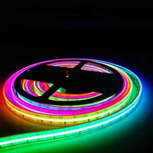
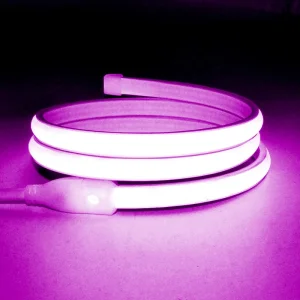
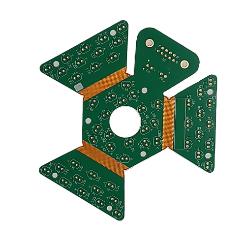
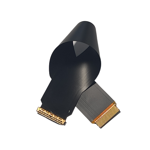
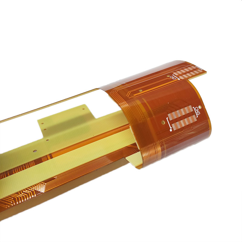
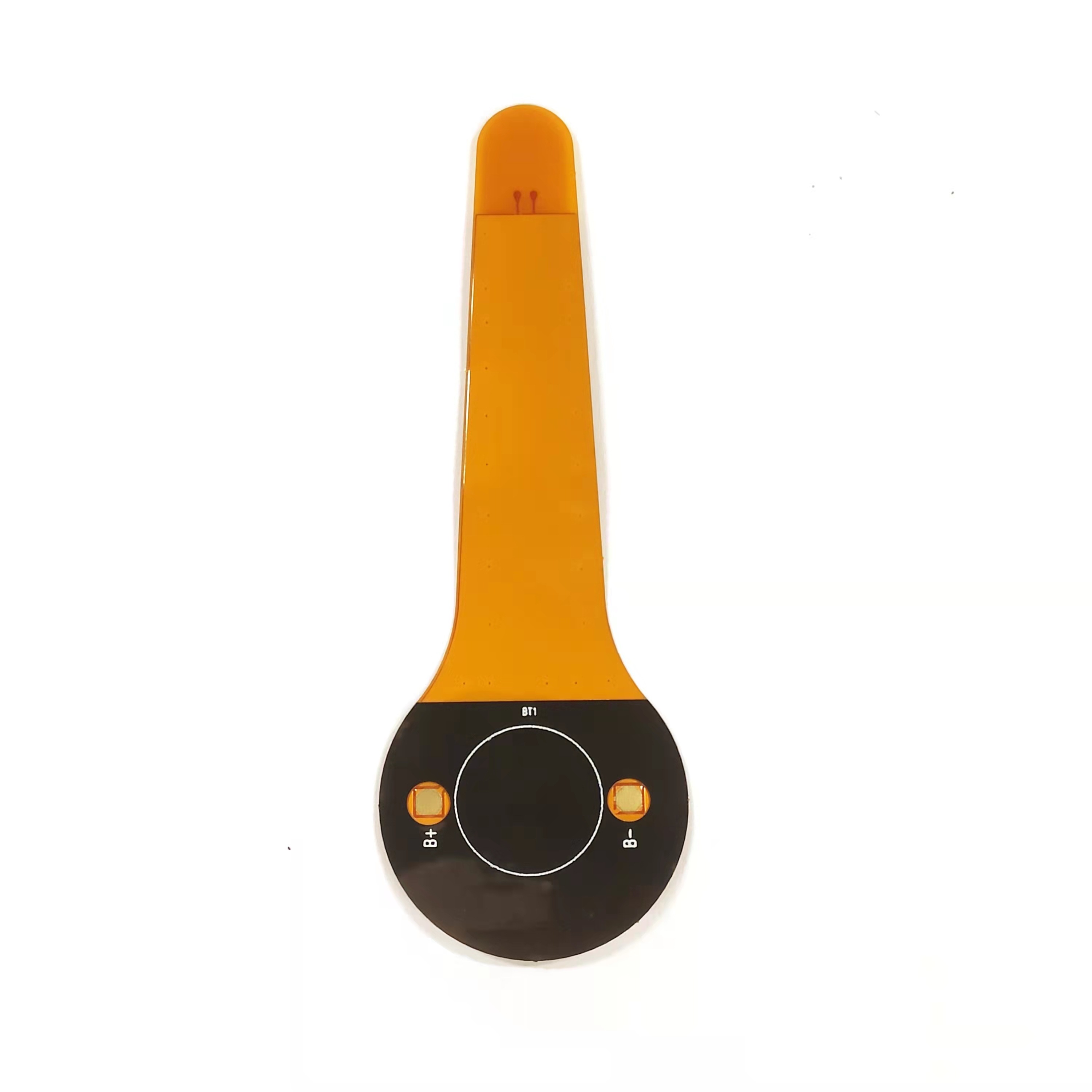
The most notable difference between rigid PCBs and flex PCBs (FPC) can be inferred from their names. Rigid PCBs are inflexible, while flex PCBs can be bent or otherwise shaped to fit inside the designated system. Flexible circuits, when designed correctly, can also be flexed for hundreds of thousands of cycles repeatedly without failure. The increased versatility of flex boards typically comes at a higher cost, but they are essential for applications with limited space requirements, such as consumer electronics, medical devices, space and automotive applications.
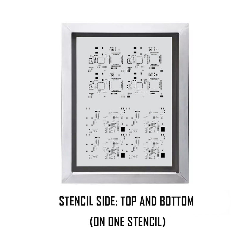
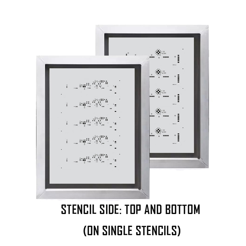
This is also a subtractive process by which removal of the laser cut stencil foil material is achieved by laser cutting. Naturally, laser cutting results in finer results and helps in achieving greater accuracy. Laser cutting also produces more consistent results than the chemical etching process. Since the process is not dependent on the chemical conditions, there is essentially no requirement for protection from moisture.
| Capability Specification | |
|---|---|
| Base Material | FR-4/High TG FR-4/CEM1/CEM3/Halogen Free material/Rogers/Arlon/Taconic/Teflon |
| Layer Count | 1-18L |
| Finished Copper Thickness | 1-6oz |
| Finished Board Thickness | 0.2-7.0mm |
| Min. Hole Size | Mechanical Hole: 0.15mm / Laser Hole: 0.1mm |
| Outline Profile | Rout/V-cut/Bridge/Stamp Hole |
| Plugging Vias capability | 0.2-0.8mm |
| Board Thickness Tolerance | ±10% |
| Board Twist & Warp | ≤5% |
| Controlled Impedance | ±5% |
| Surface Finishing | HASL/HASL lead free/ENIG( Immersion Gold)/ Immersion Tin/Immersion Silver/OSP/etc. |
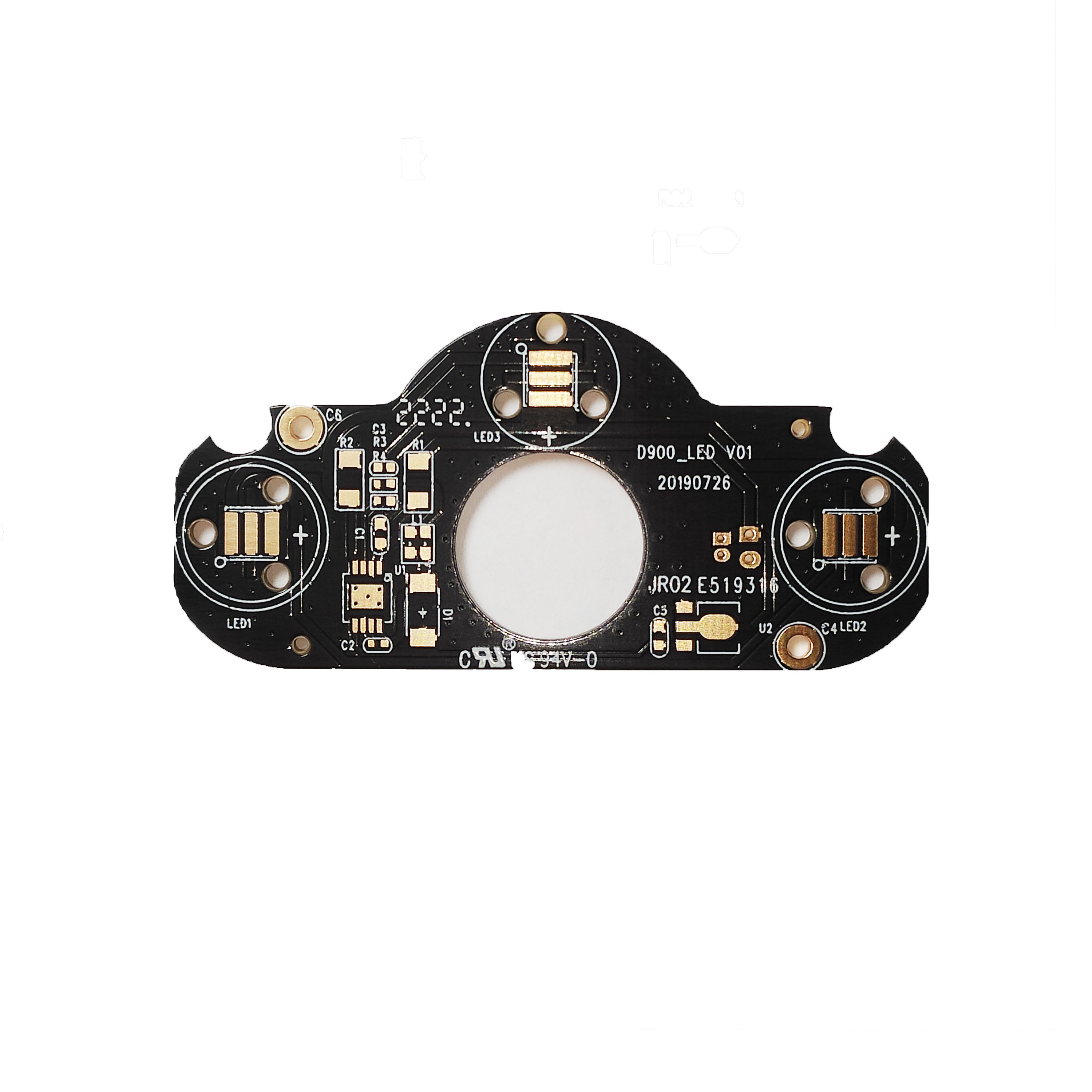
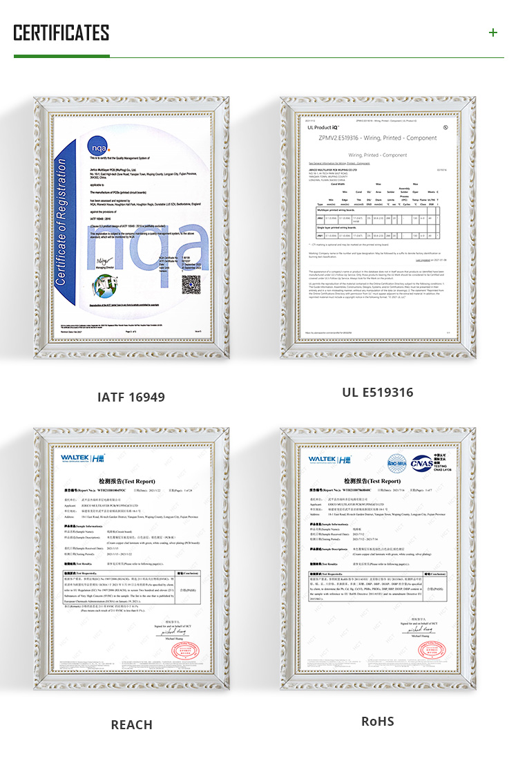
| UL Mark | E519316 |
| Lead time | 1-15 Days (Negotiable) |
| Material Identification Card | Yes |
| Inner Packaging | Vacuum Packed/ Paper Separated/ Others |
| Outer Packaging | Standard Carton Packed |
| PCB Layer Count | Quick Turn / Usual Time | Mass Production |
|---|---|---|
| 2L | 24hours / 4-5days | 7-12days |
| 4L | 48hours / 6-7days | 10-14days |
| 6L | 72hours / 7-8days | 12-16days |
| 8L | 72hours / 8-10days | 14-18days |
| 10L | 96hours / 12-14days | 16-20days |
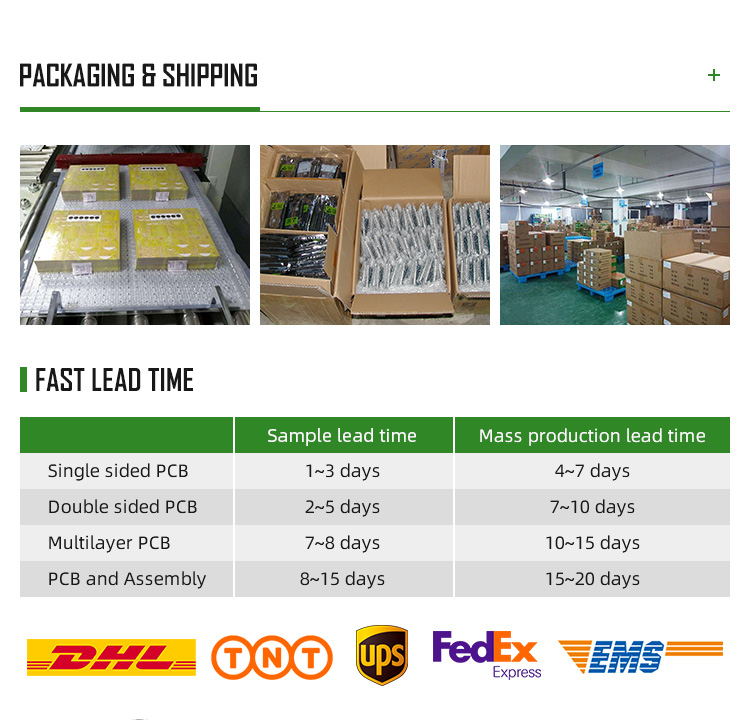
| Assembly Quantity | Usual Time |
|---|---|
| < 20pcs | 5days |
| 20-100pcs | 7days |
| 100-1000pcs | 10days |
| > 1000pcs | Depend on BOM list |
A: Gerber, Protel 99SE, DXP, PADS 9.5, AUTOCAD, and CAM350 formats are all supported.
A: Please provide the Quantity and Specifications such as material type, surface finish treatment, copper thickness, board thickness, soldermask color, silkscreen color, and any other special requirements.
A: Gerber files, a BOM (Bill of Materials) list, and pick-and-place files are required for accurate PCBA evaluation.
A: There is no MOQ. We are capable of handling both prototype small-run and large-volume productions with high flexibility.
A: For bare PCBs, we utilize Flying Probe Testing, E-testing, and automated optical inspections. For PCBA, we employ SPI, AOI, X-Ray, and final quality control (FQC) testing procedures.
A: Custom board fabrication lead times range from 1 to 15 days depending on the board complexity, layer count, and overall production volume requirements.